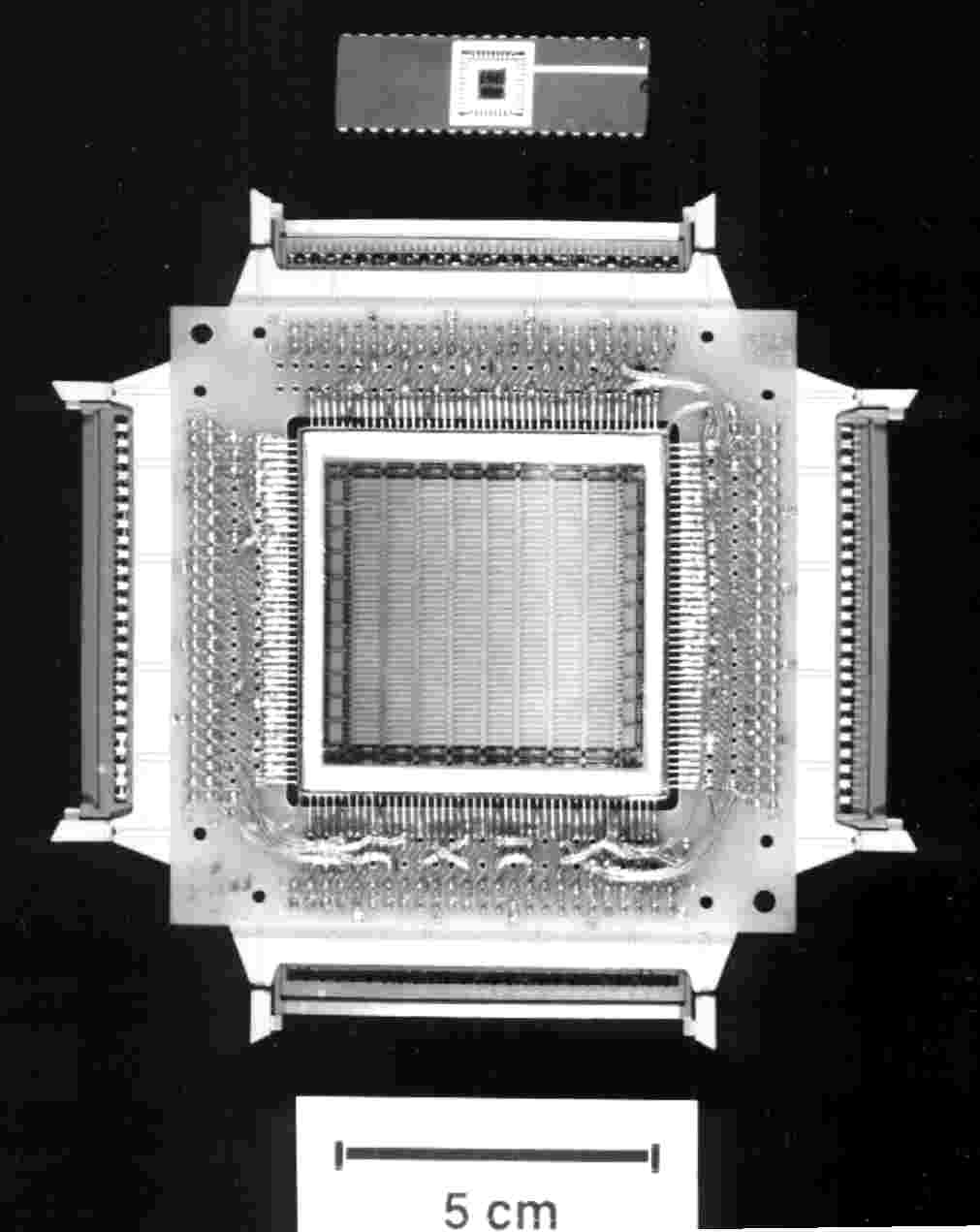
From M.I.T Lincoln Lab
Laser linking by G. Chapman,
design by M. Rhodes
| Microelectronics | Large Area/Wafer Scale Integration,
Defect avoidance techniques, VLSI design (see also Laser/Optical Applications) |
| Micromachining | Microsensors & transducers
MicroElecto-Optical Mechanical Devices |
| Laser/Optical/Sensor Applications | Laser micromachining, & Laser microsurgery,
Active Pixel Sensor Sensor Imagers Hyperspectral Sensor Systems |
| Biomedical Sensors | Laser Micromachined Biomedical Sensors |
| Space Applications | Orbital Microfabrictation,
Space based Microsensors |
| Microfabrication | Development of Inorganic Photoresists |
| Embedded Microprocessor Systems | Computer Anti-theft technology |
| Internet Anti-theft | Hardware/Software interaction with the Internet |
| This work is the creation of Large Area Restructurable Silicon System (LARSS) which involve arrays of both integrated circuits and transducers. This work aims at the creation of new silicon systems that can readily be expanded to areas and complexities much larger than current integrated circuit fabrication limits. To increase circuit area to the wafer scale level, 10-200 times the current IC area, requires defect avoidance technologies bypass IC fabrication errors and hook together working sections to create large systems. The technique divides the system into redundant circuit blocks surrounded by a grid of metal signal/clock/power bus lines to which the devices can be connected. In all cases the designs use standard IC fabrication services (eg. Canadian Microelectronics Corp.) to manufacture the devices, but applies post fabrication processing to achieve the unique systems. One interconnecting technique which makes permanent signal routing uses a laser linking system developed by the applicant at M.I.T. Lincoln Laboratory and currently applied at Simon Fraser University. It consists of two separated dopant lines in the silicon substrate which are connected to the bus lines (like a gateless transistor). An external laser melts the gap area causing the dopant lines to connect with a resistance of typically 60 ohms. The laser can also cut metal lines, thus segmenting the signal buses. |
From M.I.T Lincoln Lab Laser linking by G. Chapman, design by M. Rhodes |
In terms of work here my students and I have built a major unique piece of experimental equipment. This is a laser interconnection table which will focus a controlled laser beam on integrated circuits with a 0.1 micron position repeatability. This is one of only five such systems in the world, two at M.I.T. Lincoln Lab, plus one each at the University of South Florida and the US National Security Agency. I have played a major part in the creation of all such systems, and feel this is the best designed so far. The value of this equipment is demonstrated by the interest in using the laser table shown in the Industrial Cooperation section.
Due to the expensive nature of building true wafer scale systems my
work has concentrated on studying techniques for building large area systems
and the design of new classes wafer scale type devices. At the VLSI design
level this has resulted in building circuits to compare the area and speed
tradeoffs for defect avoidance of laser connections and active devices,
which has lead to the design of circuits combining both for optimum operation.
My research has proposed and tested a new type of large area product: the
Wafer Scale Field Programmable Gate Array which could increase the density
of current FPGA systems by 10-100 times. Another new concept was LARSS
systems containing both transducers (some micromachined), control circuitry
and the laser redundancy network needed to build in large areas. First
proposed in one of my papers, the idea here is to build large transducer
arrays using separate types of redundancy layouts for both the transducers
and the circuitry. One such systems is a large area magnetic field sensor
array designed for mapping magnetic field distributions being undertaken
by my PhD student Yves Audet. Another array was a design for a wafer scale
array of thermal emission elements. In this transducer matrixes the laser
redundancy scheme changes the design from something that can be used only
in small chip sized structures (say 10x10 arrays) to very large devices
possibly of 256 x 256, which makes it of considerable interest to several
organizations.
Click here for papers on WSI projects
Currently this wafer scale work has concentrated on the development
of large area optical sensors. (see Lasers/Optical/Sensor
Applications)
Laser micromachining is used to create unique devices not possible with current etching technology. The most import work here is a vision/proximity sensor called "Vision Skin" developed by myself and my grad students for the Canadian Space Agency. Vision Skin gives both gives a low resolution image of the an approaching object and measures the distance to it with precision 100 micron precision. This patented device has been licensed by the Canadian Space Agency and Kinetic Sciences Inc. Click here for papers on the Vision Skin project This is part of the Angular Domain Imaging work (see the Biomedical Sensor section)
In addtion to the laser links a Laser Microsurgery on Integrated Circuits
service for Canadian Microelectronic Corp. members has been offered using
my laser table during the past four years. Removing defects occurring in
chip designs has been done for researchers directed to this laboratory
by CMC. Specifications for this service is maintained by CMC on their web
site. The most important and successful project consisted of a nearly 8
months project with McGill's Electronic department. A very large IC, consisting
of about 40% of the area of a CMC 1.2 micron fabrication run, contained
several design defects which made them totally inoperable. The size of
the chip meant that it would be very expensive to refabricate. In a series
of experiments involving the exchange of 5 sets of chips the problems were
identified by successive cut and test cycles. The final work produced fully
operable devices, enabling the student to obtain his thesis. Several local
companies have used this laser microsurgery to analyze problems with their
chips and reduce the design cycle.
A unique UV laser micromachining facility has been funded by Canadian
Foundation for Innovation grant and is currently being built up in our
lab. This will be used to build biomedical devices cooperative research
with two companies. These consist of precisely shapped plastics holding
patterns of electrodes which make contact to the nerves. We build these
by an ultraviolet (UV) laser on a computer controlled micropositioning
table to create 3D structures with photoablation: where the UV photon's
energy literally tears apart the molecules of plastics and allows the automated
shaping of materials. The computer controlled UV laser table system will
allow cuff design and electrode positions to be altered from one test sample
to another, for rapid design evolution.
Bimetallic thermal alloying resists consist of two thin metal films.
In and Bi, in this case, are RF or DC sputtered to the thickness of 15-150
nm on a thin film layer that is going to be patterned. When exposed to
light under a photomask, as shown in, the material in the exposed area
will absorb the light energy and be heated up to above the Bi/In eutectic
temperature. Since the alloy has a lower melting point than either individual
film, melting will begin at the interface between the two layers and move
outward as the melt pool grows. At the end of the laser pulse, the
resist layers will cool and solidify as the eutectic alloy. The material
in the unexposed area, where the light is blocked by the photomask, will
remain the same as two-layer structure. Tests show that the alloy have
different chemical properties from Bi or In. For the resist development
after exposures, two etch solutions have been found which will attack the
areas of unexposed resist more aggressively than the exposed areas. After
the resist development, the alloyed area remains while the unexposed area
is removed. The pattern is then transferred to the underneath layer to
be patterned by plasma etching or wet etching. After the resist stripping,
the whole lithography process is completed.This project is supported by
a grant from CREO Products, the BC Advanced Systems Institute and BC Science
Council.
Click here for papers on the Inorganic
Resist project
The potential advantage of Microfabrication in space has been under
study by my research team at Simon Fraser University. The project
was first conceived in 1990 during my period on the research staff of Massachusetts
Institute of Technologys Lincoln Laboratory microelectronic group where
I was principal researcher on the Restructurable Wafer Scale Integration
project. The project proceeded at a modest level, with a first publication
in 1991 while the questions were considered. Starting in 1998 Boeing
Aircraft funded a more intense research phase was entered which culminated
in a Masters project by Nick Pfeiffer. This carefully investigated
the main technical problems, issues, costs and benefits of space.
Studies showed that successful space microfabrication needed to change
the existing wet organic photoresist process for a vacuum based dry resist
process. Several such process to do this have been proposed in the
literature.
Click here for papers on space microfabrication
Howver, one of the considerable synergies of our work is the development
under a separate program of a Inorganic Dry thermal resist for CREO Products,
a world leader in applications of organic thermal resists. (see
Microfabrication section)
Another space related project is the Vision Skin proximity and imaging
sensor work is continuing in a cooperative program with the Canadian Space
Agency. See the Laser/Optical Sensors area.